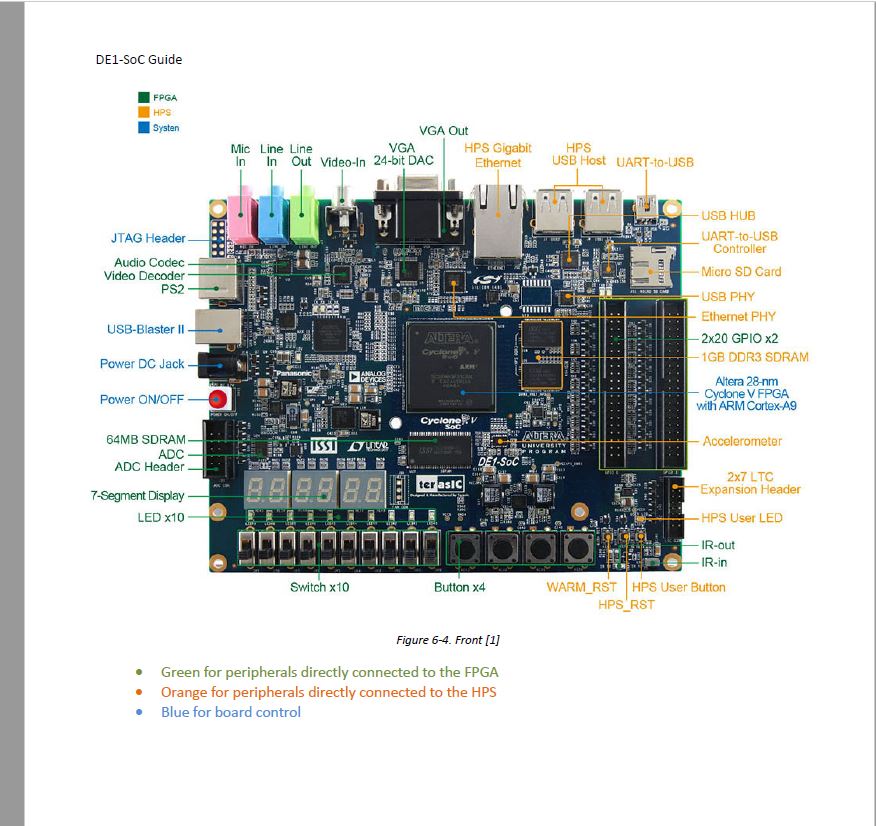
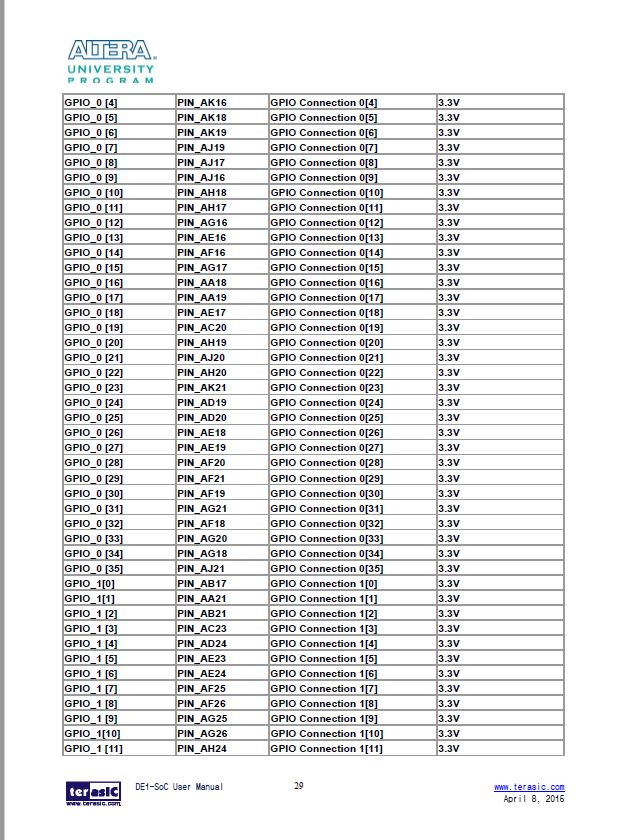
GPIO 0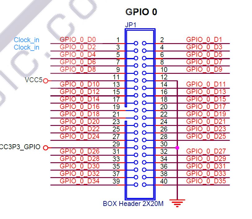
Note: The pin numbers are misleading: CPIO_0_D0 is actually Pin 0 in the FPGA pin assignment (not 1)
GPIO_0_D0 would be FPGA pin PIN_AC18
GPIO_0-D1 would be FPGA pin PIN_Y17
GPIO 1
Note: The pin numbers are misleading: CPIO_1_D0 is actually Pin 0 in the FPGA pin assignment (not 1)
GPIO_1_D0 would be FPGA pin PIN_AB17
GPIO_1_D1 would be FPGA pin PIN_AA21
GPIO Header 1
GPIO_0[0] PIN_AC18 through GPIO_0[35] AJ21
 GPIO Header 2
GPIO_1[0] Pin AB17 through GPIO_1[35] AC22
J2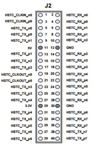
180-pin Female HSTC Connector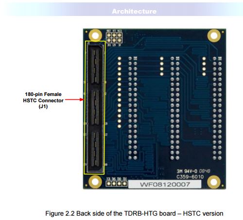
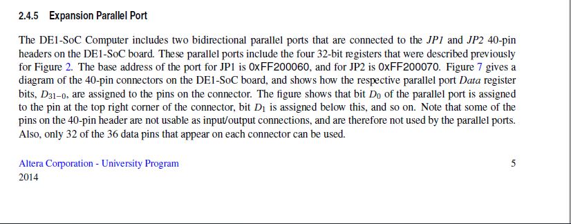
GPIO Pin Assignment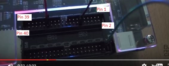
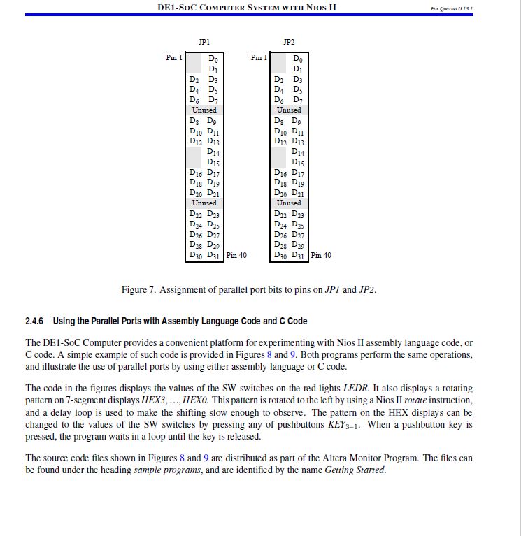
Following images from the DE1-SoC-Computer.pdf; access from Monitor Program "Documentation"
I believe that the four "unused" sections are +5 and ground, in pairs
Source "C" Language code for accessing the LEDs
Note: various sources state that a 40-pin IDE/ATA type ribbon cable has pin1 as Reset and pin40 as ground
Content from "default" monitor program sof (
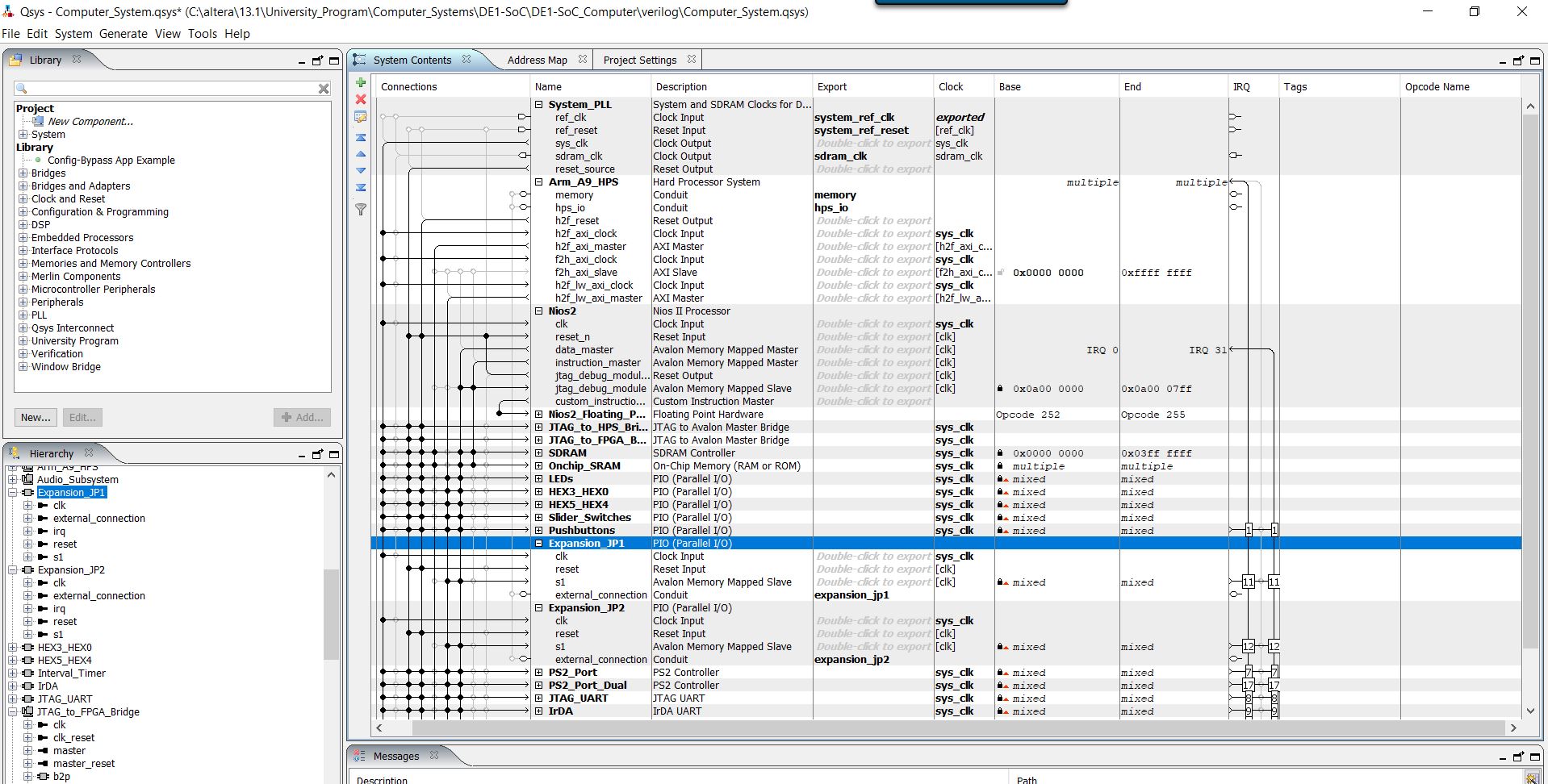
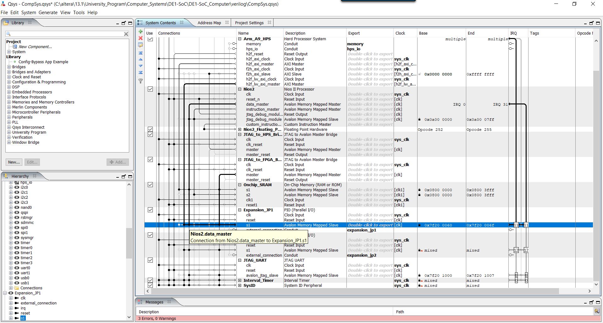
Note: these two images are a modified version of Computer_System.qsys; elements removed for clarity.
Arm_A9_HFS.h2f.lw_axi_master
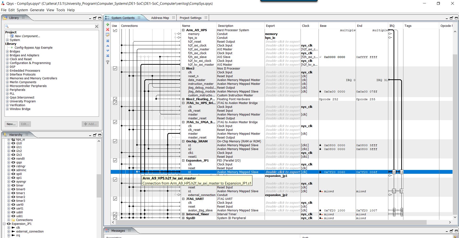
Nios2.data_master
When comparing the pin numbers on the 40-Pin header expansion, it is mirrored from the pin numbers on the 40-pin ribbon cable.
Note: For the header expansion, pin 1 is the upper right pin
Also, the Data and GPIOpins listed below exclude the "extra" pins such as the +5 volt and ground pins
| Note: These are for the GPIO J1 | ||
| GPIO Mask (hex) | GPIO pin number | Data number (from figure 7 above) |
| 0x1 | pin 1 | D0 |
| 0x2 | pin 2 | D1 |
| 0x4 | pin 3 | D2 |
| 0x8 | pin 4 | D3 |
| 0x10 | pin 5 | D4 |
| 0x20 | pin 6 | D5 |
| 0x40 | pin 7 | D6 |
| 0x80 | pin 8 | D7 |
| 0x100 | pin 9 | D8 |
| 0x200 | pin 10 | D9 |
| 0x400 | pin 11 | D10 |
| 0x800 | pin 12 | D11 |
| 0x1000 | pin 13 | D12 |
| 0x2000 | pin 14 | D13 |
| 0x4000 | pin 15 | D14 |
| 0x8000 | pin 16 | D15 |
| 0x10000 | pin 17 | D16 |
| 0x20000 | pin 18 | D17 |
| 0x40000 | pin 19 | D18 |
| 0x80000 | pin 20 | D19 |
| 0x100000 | pin 21 | D20 |
| 0x200000 | pin 22 | D21 |
| 0x400000 | pin 23 | D22 |
| 0x800000 | pin 24 | D23 |
| 0x1000000 | pin 25 | D24: Not working |
| 0x2000000 | pin 26 | D25: Not working |
Results for GPIO J2: Tested for D0; worked!
Here's the test program for the above (using the Monitor "test program" project) TestComputer.c
Resources for "bare-metal" programming:
Memory Layout diagram
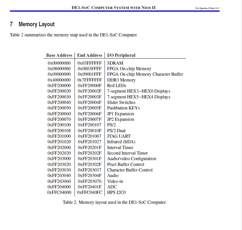
NOTE: The green represents hardware directly connected to FPGA, orange directly connected to HPS;
The GPIO two connectors are directly controlled by the FPGA!
8.3.2 Application Over an Operating System (Linux)
Running code over a linux operating system has several advantages. First of all, the kernel releases CPU1 from reset upon boot, so all processors are available. Furthermore, the kernel initializes and makes most, if not all HPS peripherals available for use by the programmer. This is possible since the linux kernel has access to a huge amount of device drivers. Multi-threaded code is also much easier to write, as the programmer has access to the familiar Pthreads system calls. Finally, the linux kernel is not restricted to running compiled C programs. Indeed, you can always run code written in another programming language providing you first install the runtime environment required (that must be available for ARM processors).
However, running an “EMBEDDED” application on top of an operating system also has disadvantages. Due to the virtual memory system put in place by the OS, a program cannot directly access the HPS peripherals through their physical memory-mapped addresses. Instead, one first needs to map the physical addresses of interest into the running program’s virtual address space. Only then will it be possible to access a peripheral’s registers. Ideally, the programmer should write a device driver for each specific component that is designed to have a clean interface between user code, and device accesses.
At the end of the day, bare-metal applications and applications running code on top of linux can do the same things. Generally speaking, programming on top of linux is superior and much easier compared to bare-metal code, as its advantages greatly outweigh its drawbacks.
      8.4 GOALS
Let’s start by defining what we want to achieve in this tutorial. We want to create a system in which both the HPS and FPGA can do some computation simultaneously. More specifically, we want the following capabilities:
1. A Nios II processor on the FPGA must be able to use the 10 LEDs and 10 switches connected to the FPGA PORTION of the device. The Nios II processor will create a strobing light effect on the 10 LEDs, with the 10 switches acting as enable signals for the corresponding LEDs.
2. The Nios II processor will use its SDRAM instead of any form of on-chip memory.
3. The HPS must be able to use the LED and button that are directly connected to the HPS PORTION of the device. Pressing the button should toggle the LED.
4. The HPS must be able to use 2 buttons and the six 7-segment displays connected to the FPGA PORTION of the device. The HPS will increment and decrement a counter that will be shown on the 7-segment displays. Pressing the first button should invert the counting direction, and pushing the second button should reset the counter to 0.
5. The HPS must be able to use the ethernet port on the board.
6. The HPS must be able to use the microSD card port on the board to which we will write anything we want.
Note: The two buttons the six 7-sements displays are connected to the FPGA portion!
Color-Coded Board Layout