
Important Terms and Definitions
- 1 hertz
- 1 second
- 1 KiloHertz
- .001 second
- 10 KiloHertz
- .0001 second
- 100 KiloHertz
- .0001 second,1.0E-5
- 1 MegaHertz
- .00001 second,1.0E-6
- 10 MegaHertz
- .000001 second,1.0E-7
- 50 MegaHertz
- .0000002 second,2.0E-8, 20 nano seconds
- 100 MegaHertz
- .0000001 second,1.0E-8
- 38kHz
- 26.3µs
- AXI
- Advanced eXtensible Interface
- bdf
- Block Design File
- HDL
- Hardware Description Language
- HPS
- Hard Processer System
- HSTC
- High-Speed Terasic connector/dd>
- HSMC
- High-Speed Mezzanine connector
- lpm
- Library of Parameterized Modules
- lsb
- Least Significant Bit
- qsf
- Quartus II Settings File
- qpf
- Quartus II Project File
- msb
- Most Significant Bit
- PLL
- Phase-Locked Loop
- sof
- SRAM Object File
- sdc
- Synopsys Design Constraints File
- sym
- Symbol File
- JIC
- JTAG Indirect Configuration File
DE1-SoC My First FPGA PDF manual
Design Flow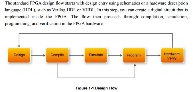
Finished screenshot of My First Fpga bdf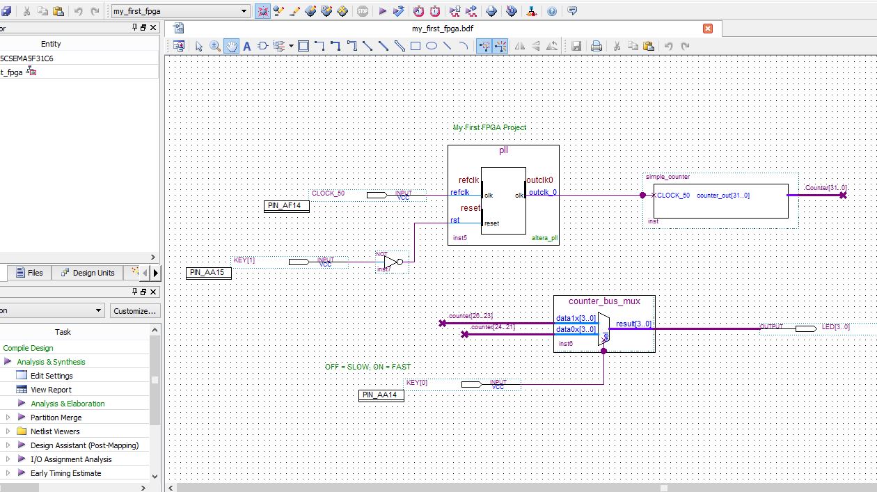
Pin Planner Top View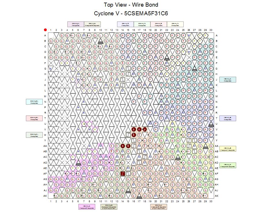
All directions are for use with the above manual
- Recommend using NO spaces within element names; i.e.: counter[26..23]
- bus name notation is [X..Y]
- X is the most significant bit, MSB
- Y is the least significant bit, LSB
- NOTE: The following files are for your trouble-shooting use only!
- Simple Counter bsf file
- Simple Counter v file
Sample instructions for creating SOF
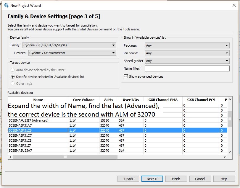
- File > New Project Wizard
- Select device: 5CSEMA5F31C6
- File > New > Block Diagram/Schematic File
- File > New > Verilog HDL File
- Select File > Save As [simple_counter.v]
- Enter code into new "file.v"
- File > Save
- File > Create/Update > Create Symbol Files
- click Add Symbol on the toolbar, select Megawizard Plug-in Manager
- Place symbol on the bdf tab
- Processing > Start > Start Analysis & Elaboration
- Assignments > Pin Planner
- Tools > TimeQuest Timing Analyzer
- File > New SDC file
- enter commands; File > Save as my_first_fpga.sdc
- Start Compilation
- [plug in DE1-SoC board, connect USB-Blaster II connector to J13, and USB cable to PC]
- Tools > Programmer
- Click Auto Detect
- Select 5CSEMA5 and click OK
- Select SCSEMA5F31; click Change File
- Note: the FPGA is the SCSEMA5 icon
- Note: the HPS is the SOCVHPS icon
- Click on Program/Configure tab
- Press Start button
- Press and hold KEY[0] make LEDs advance quicker
Image showing USB Blaster-II and power connection to DE1-SoC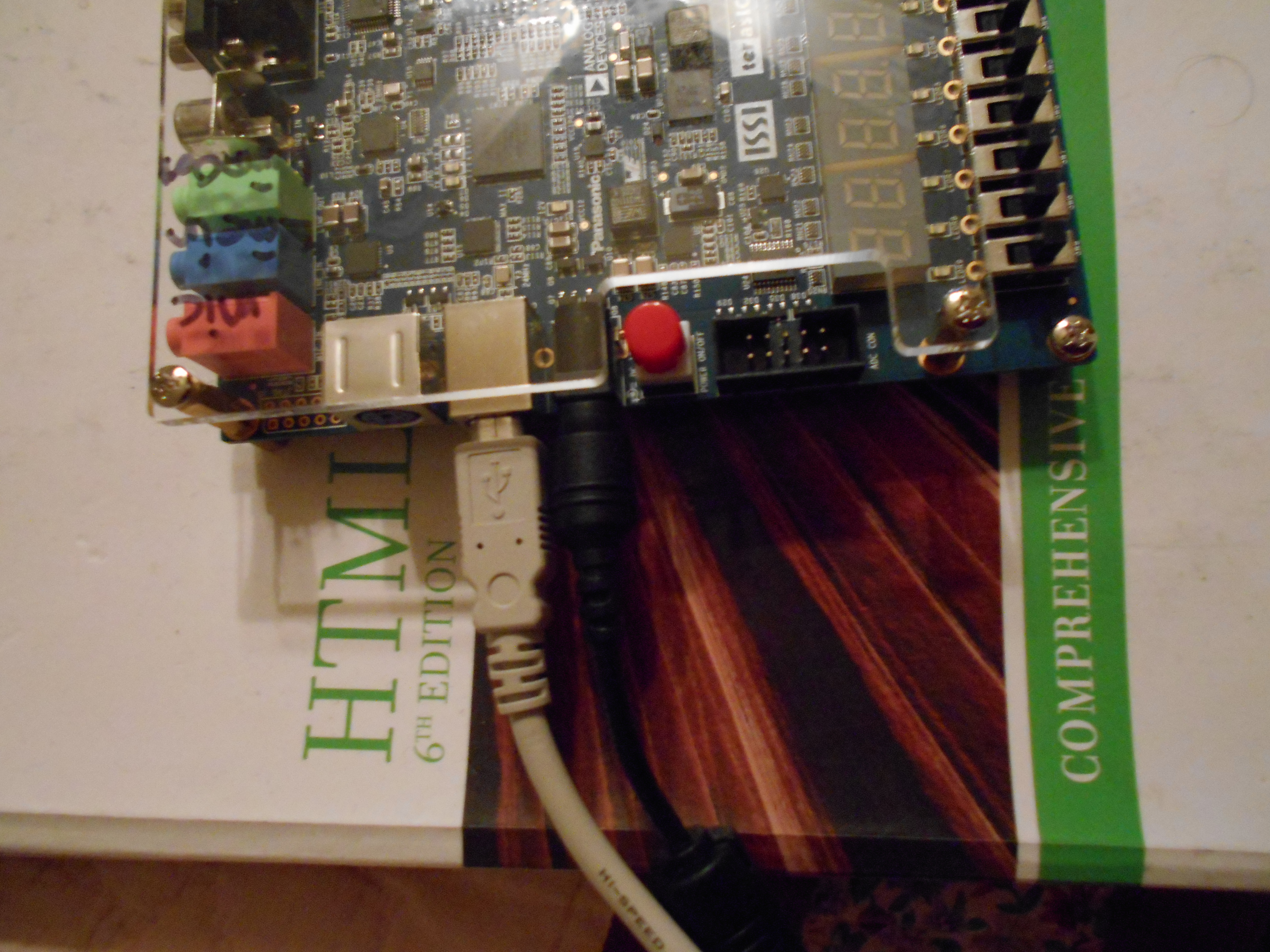
Assign DE1-SoC Hardware, Download SOF, and Program Device mp4 Video
Assign DE1-SoC Hardware, Download SOF, and Program Device Video