Table 3-5 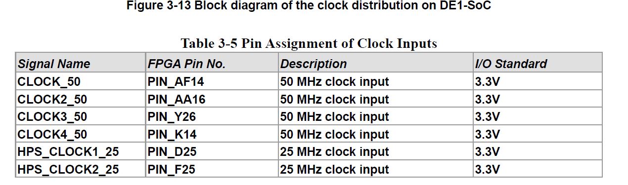
Table 3-6
Note: re: "DE1-SoCUserManual", when the switch is in the down position (towards the edge of the board), it generates a low logic
level to the FPGA.
When the switch is set to the UP position, a high logic level is generated to the FPGA.
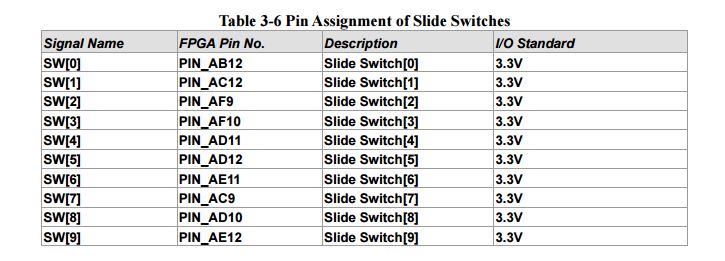
Image depicting SW0 as closed 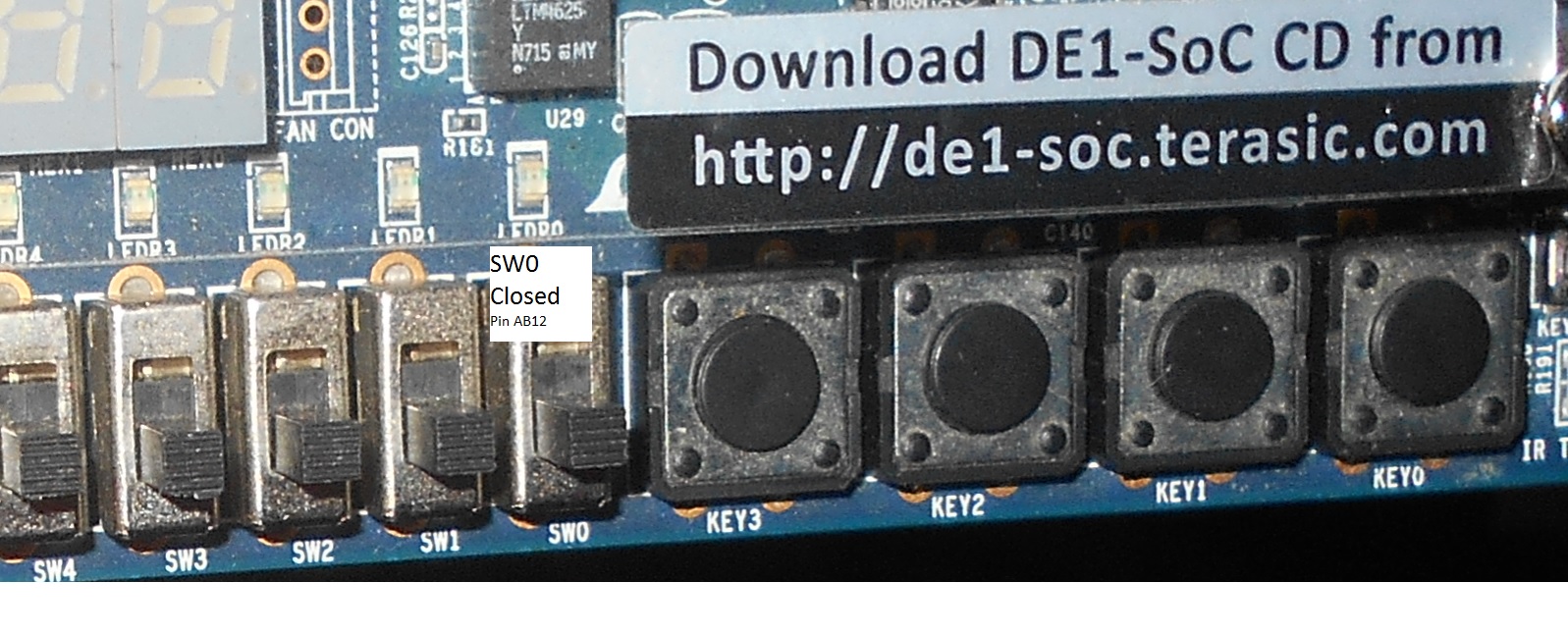
Table 3-7 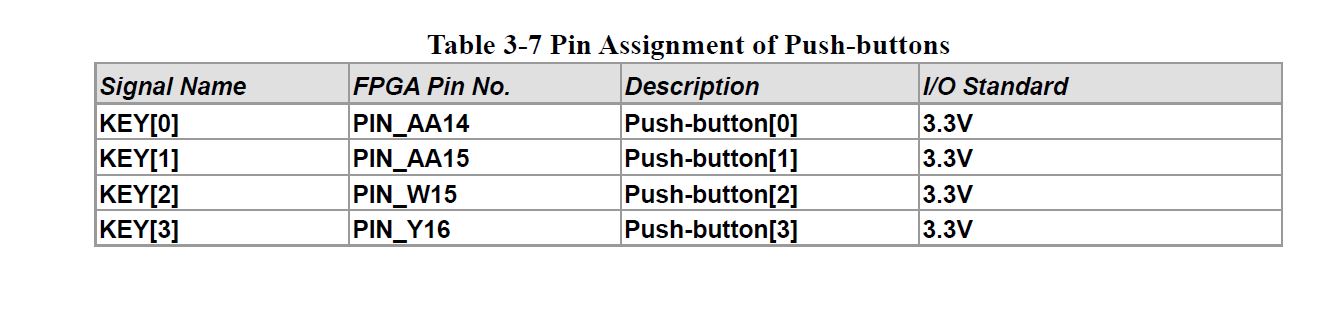
Table 3-8 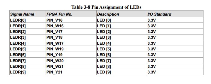
Table 3-9 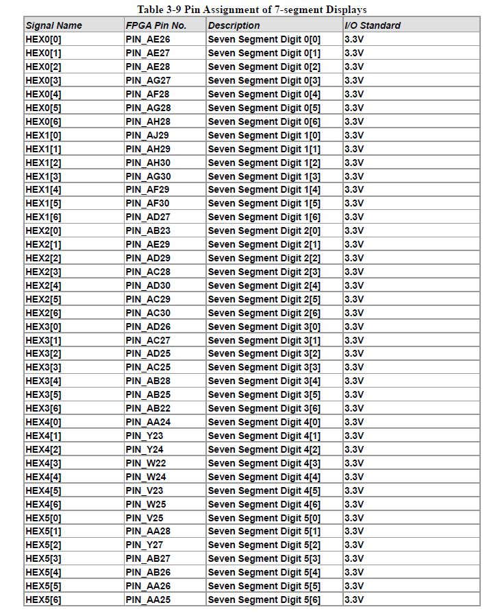
Table 3-11
Note: Ground is 6th pin (starting from 1), on the right side
VCC5 is the 6th pin (starting from 1), on the left side
Both of these pins do NOT have a FPGA pin assignment
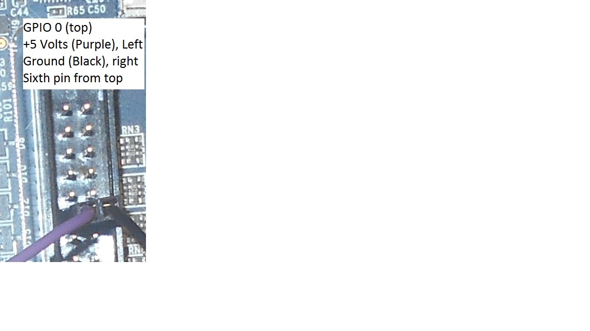
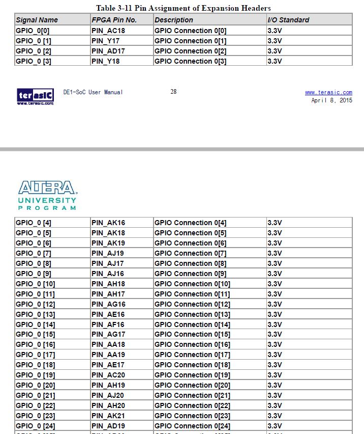
Table 3-11
Note: Ground is 6th pin (starting from 1), on the right side
VCC5 is the 6th pin (starting from 1), on the left side
Both of these pins do NOT have a FPGA pin assignment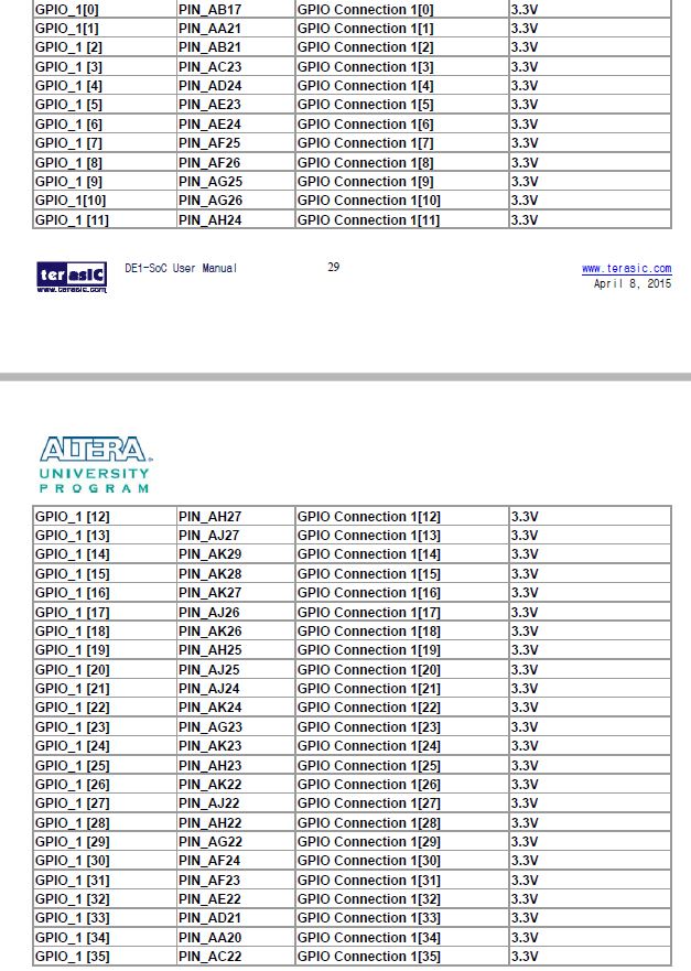
Table 3-12 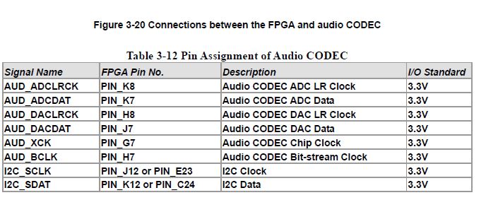
Table 3-13 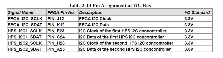
Table 3-16 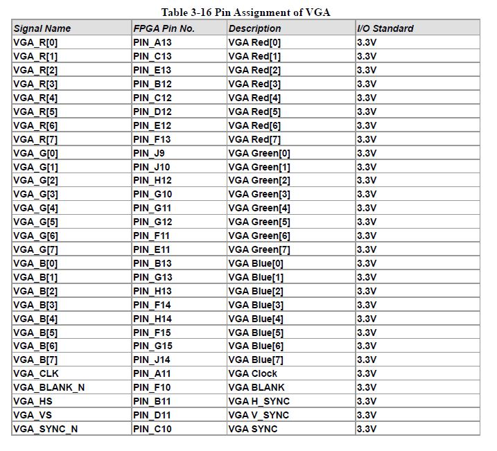
Table 3-17 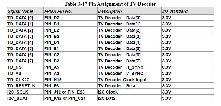
Table 3-18 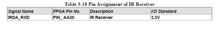
Table 3-19 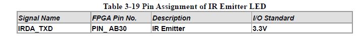
Table 3-20 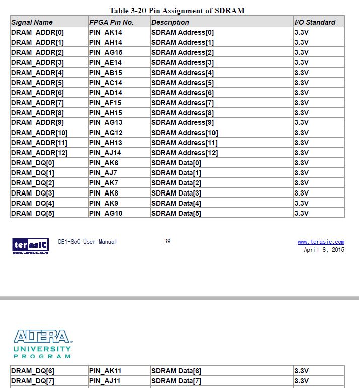
Table 3-21 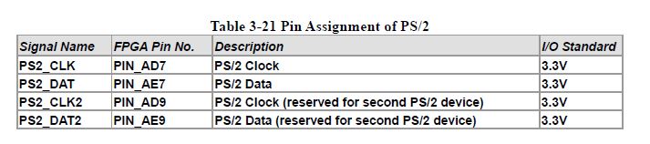
Table 3-22 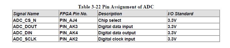
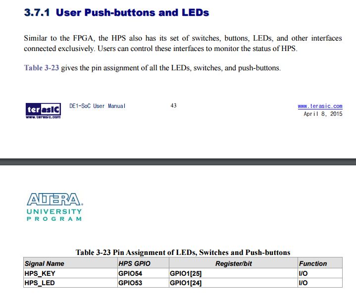
Table 3-23