Switch Gpio
- File | New Project Wizard
- name of this project? SwitchGpio
- Click on "next"
- Click on "next"
- Device family: Cyclone V, Devices: Cyclone V SE Mainsteam
- Click on 5CSEMA5F31C6, then select "finish"
- File | New | Block Diagram/Schematic File
- File | Save as SwitchGpio.bdf
- Note: Press "Escape" to turn off selected primitive
- Click on "Pin Tool"
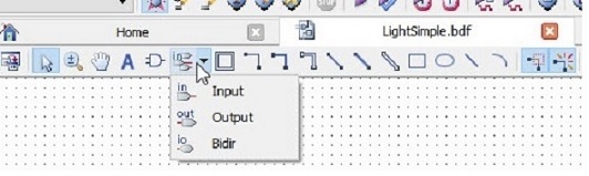
- Select "input", place in center of grid

- Note: While the input is selected, use the cursor keys to make small adjustments within the grid
- Click on "Pin Tool"
- Select "output", place in center of grid
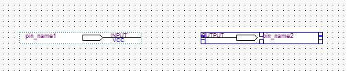
- Double click on each default name for pin; left one is SW0; right is Pin1
- Extend input pin to the left side of output; make sure the connector icon is visable
- Note: If your connecting line extends too far, click on it, then right click and choose delete; pressing the delete key does not work
- Optional: Using the "A" symbol, annotate the grid
- Click on the Save icon
- File | Create/Update | Create HDL Design File from Current File
- File Type: VHDL
- File | Open "vhd" file just created
- File | Create/Update | Create Symbol Files for Current File
- Processing | Start Compliation
- Choose "Assignments | Pin Planner"
- Using the values above, select the proper locations for each pin
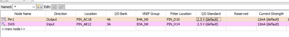
- SW0: LOC PIN_AB12
- Pin1: LOC Pin_AC18
- Close out Pin Assignment module
- Tools | Programmer
- Click on "Auto Detect"; select 5CSEMA5 and click "OK"
- Double click on 5CSEMA5, select SOF from output_files
- Click on "Program/Configure"; click on "Start"
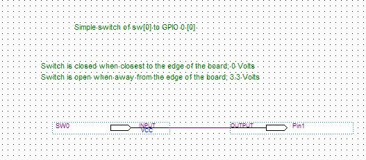
Results of downloading and observing the GPIO 0 [pin 1] with an Osilloscope with the switch off, Voltage 0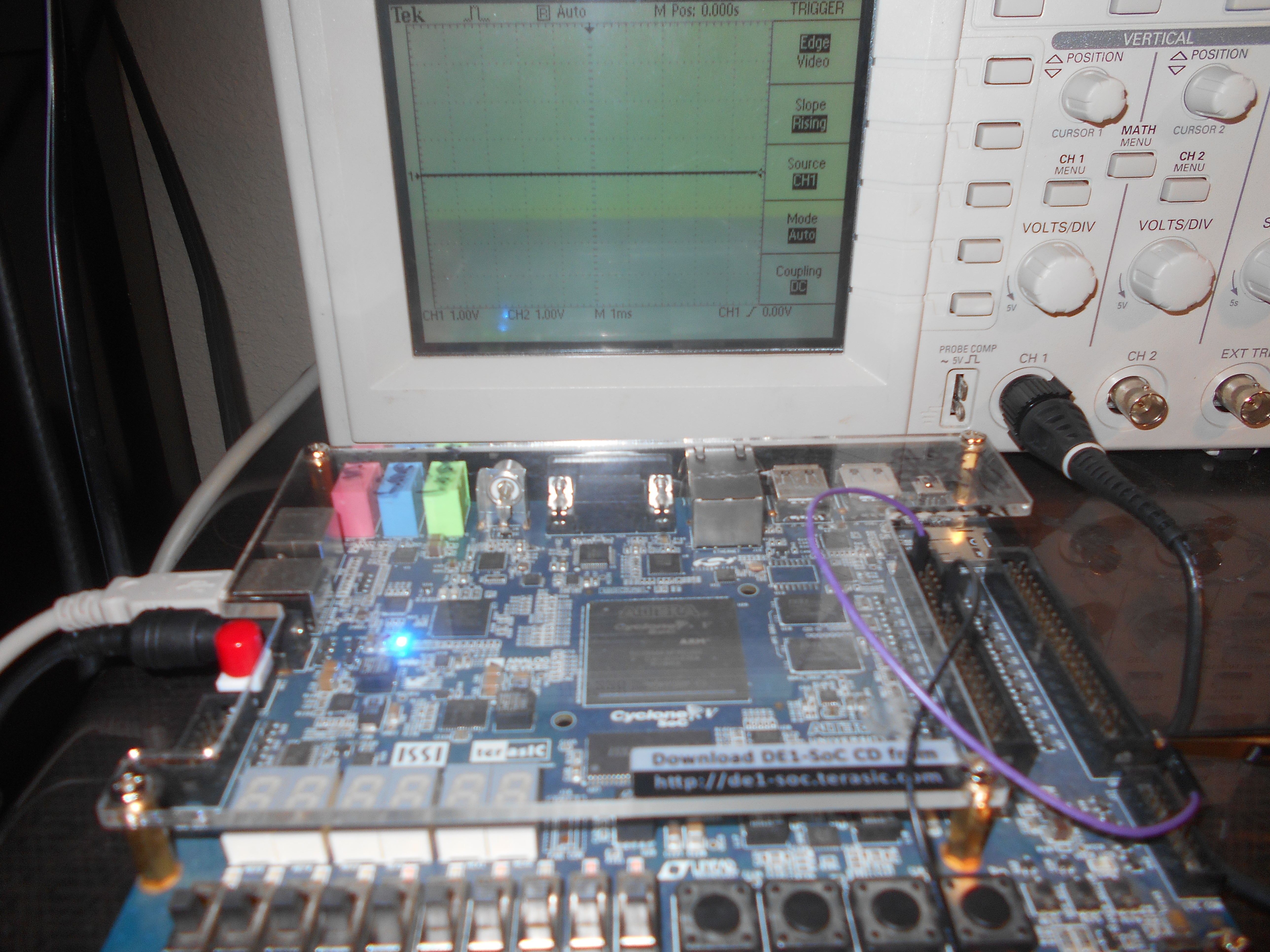
Here the SW0 is on, Voltage around 3.5 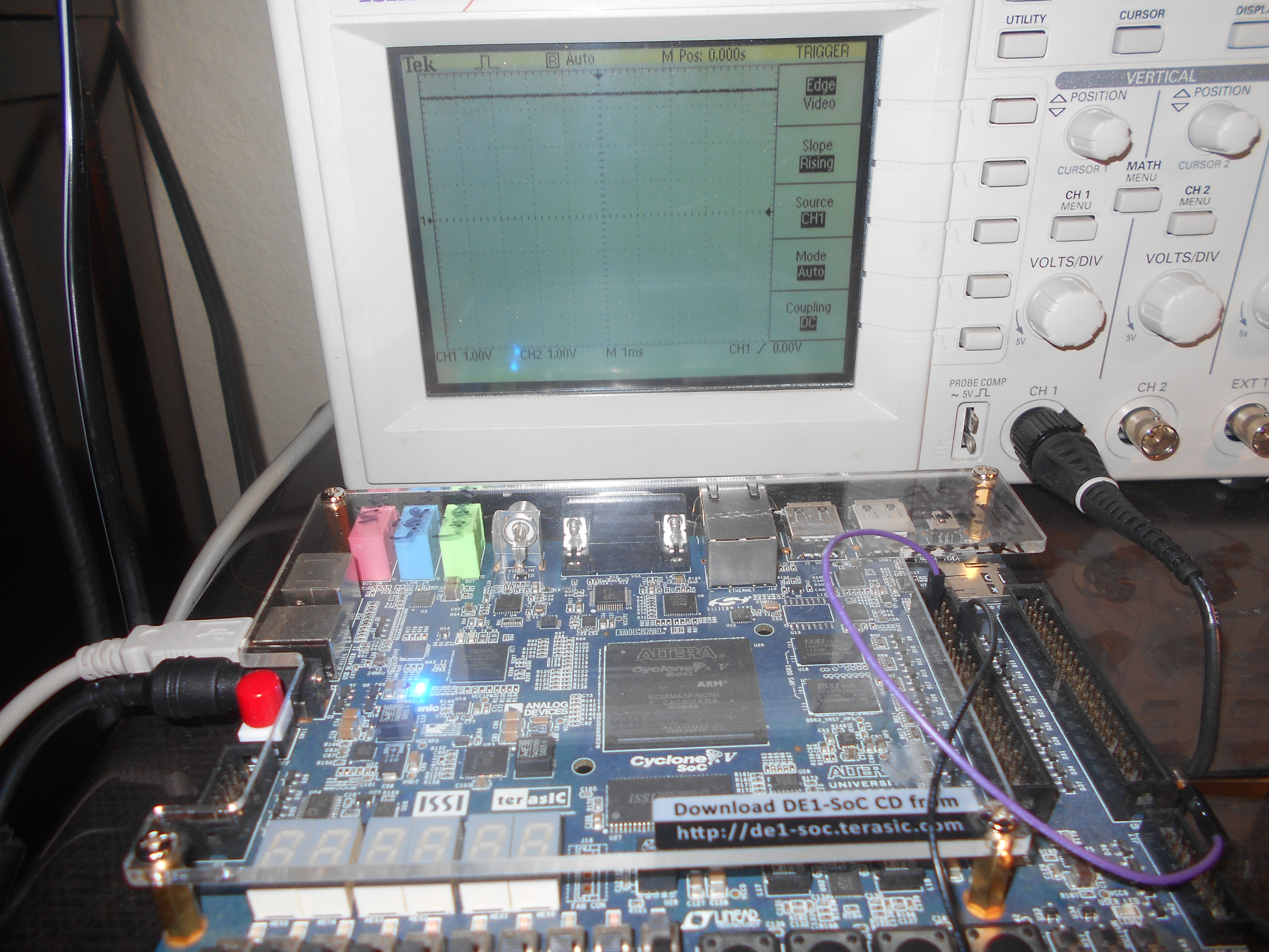
Results, shown by O-Scope, switching SW0 on and off
Return to Projects Section
